

Jakarta, Komite.id – In his keynote, Jensen Huang introduced NVIDIA NVLink Fusion, a new class of super switch technology designed to deliver ultra-high bandwidth communication between GPUs and memory.
NVLink Fusion is a breakthrough interconnect architecture that enables NVIDIA’s partners—regardless of their system design—to scale up AI infrastructure efficiently. The solution empowers hyperscalers to build semi-custom compute systems optimized with NVLink, enhancing flexibility and performance.
This next-generation technology is engineered to eliminate traditional east-west traffic bottlenecks within data centers, unlocking a new level of scalability for AI workloads. It supports the evolution of the AI Data Center and AI Factory, enabling more flexible and efficient system architectures tailored to specific AI needs.
“This incredible body of work is now flexible and open for anyone to integrate,” said Huang.
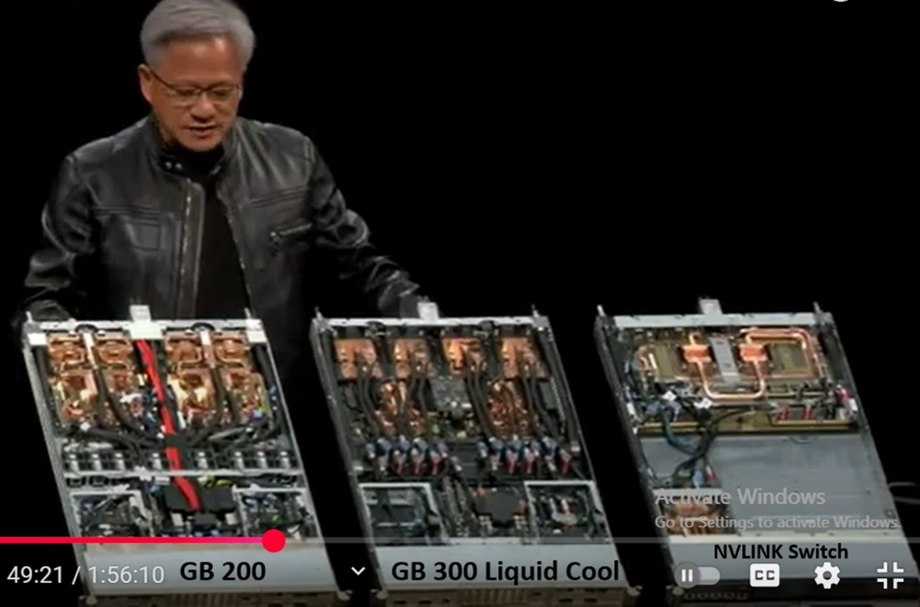
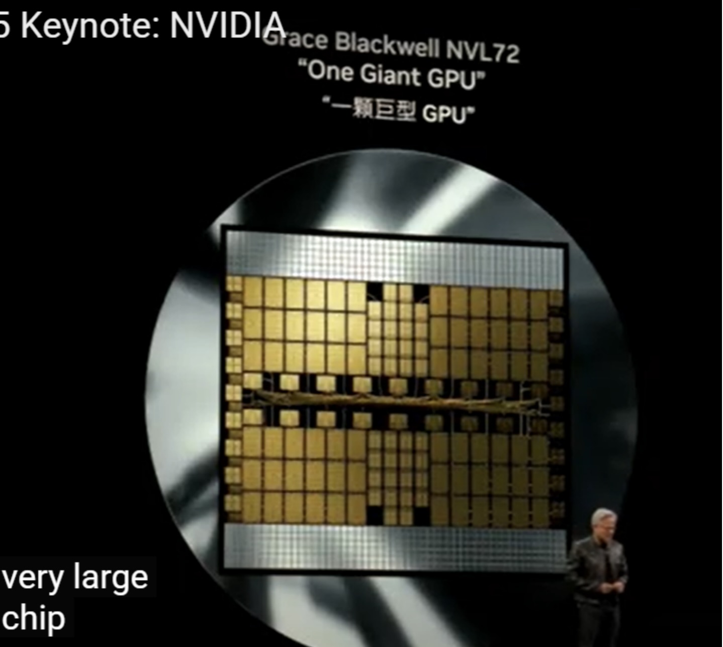
In the case of Blackwell, NVIDIA even connected 2 supercomputer chip together to make it possible and to achieve scale up. TSMC worked with NVIDIA to create these giant chip or scale up.
But still Jensen dream of chips way bigger than that. And so NVIDIA had to create what is called NVlink Switch or the world fastest switch at 7.2 Terabyte per second. Nine of these Switches are going into the Blackwell Rack.
In the case of Blackwell, NVIDIA went a step further by connecting two supercomputer-class chips together, enabling unprecedented scale-up capabilities. To make this possible, TSMC collaborated with NVIDIA to manufacture these massive chips designed specifically for high-performance AI workloads.
Yet, Jensen Huang envisions chips even larger and more powerful than what currently exists. To support this vision, NVIDIA developed the NVLink Switch—the world’s fastest interconnect switch, capable of delivering 7.2 terabytes per second of bandwidth.
Each Blackwell Rack incorporates nine of these NVLink Switches, forming the high-speed fabric that allows GPUs to communicate seamlessly at scale.
NVLink Spine: The Backbone of the System
The nine NVLink Switches are interconnected by a 70-pound engineering marvel known as the NVLink Spine, which contains 2 miles of cable. This spine includes over 5,000 impedance-matched coaxial cables, enabling seamless communication between all 72 GPUs through the NVLink Switches, delivering an incredible 130 terabytes per secondof total bandwidth.
To put this into perspective: the peak traffic of the entire global Internet is approximately 900 terabytes per second. Divide that by 8, and you’ll find that the NVLink Spine carries more data than the entire Internet.
With this single NVLink Spine linking all nine switches, every GPU can communicate with every other GPU simultaneously, with no compromise in speed or performance. This is the true miracle of the GB200 architecture. In electronic systems, there is a physical limit to how far a signal can travel through a circuit while maintaining performance. With GB200, this architecture pushes that limit further than ever before—from chip, through the switch, up to the NVLink Spine, and back down to any other chip.
Because of this limit, NVIDIA had to place everything within a single rack, and that rack consumes 120 kilowatts of power. That’s why the entire system must be liquid-cooled—air cooling simply isn’t sufficient at this scale. Thanks to NVLink Switch technology, we now have the ability to disaggregate GPUs from a single motherboard and extend them across an entire rack. Effectively, the entire rack functions as one massive motherboard—and that’s the true breakthrough.
With this achievement, we can now scale up compute power within a single system—and then scale it out into massive distributed supercomputers. Almost everything NVIDIA builds today is gigantic. That’s because NVIDIA isn’t just building servers or data centers—NVIDIA is building full-scale AI factories.
“This picture features CoreWeave, a $1.6 billion NVIDIA-powered supercomputing data center, recognized as one of the fastest in the world.”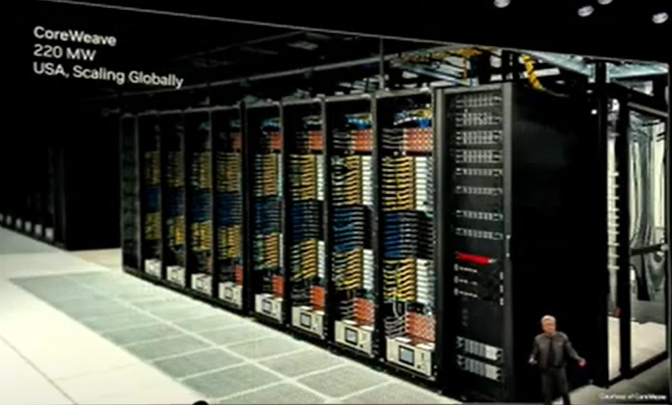
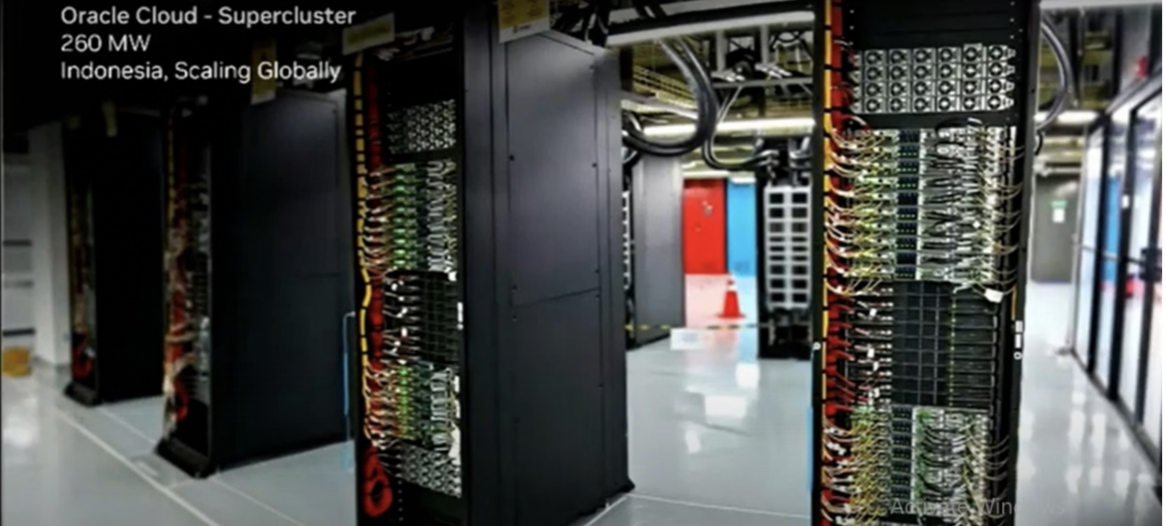
“The 220MW data center in Plano is a remarkable feat of engineering. Meanwhile, the image also showcases Oracle Cloud’s 260MW Supercluster built for Indonesia. Due to the extremely high power density per rack, the systems are spaced further apart to allow effective power distribution through liquid cooling.
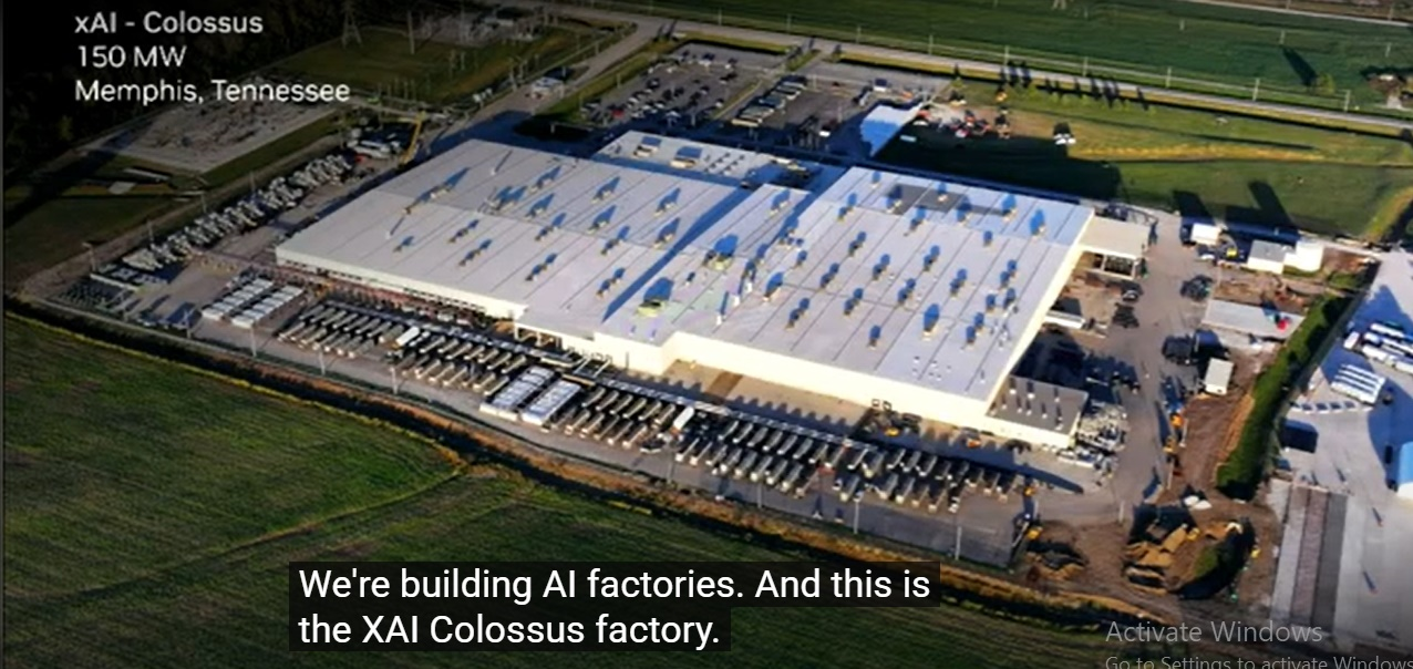
Additionally, this picture features the 150MW XAI Colossus Factory in Memphis, Tennessee — built by Elon Musk for X (formerly Twitter) to power Grok, his next-generation AI initiative.”
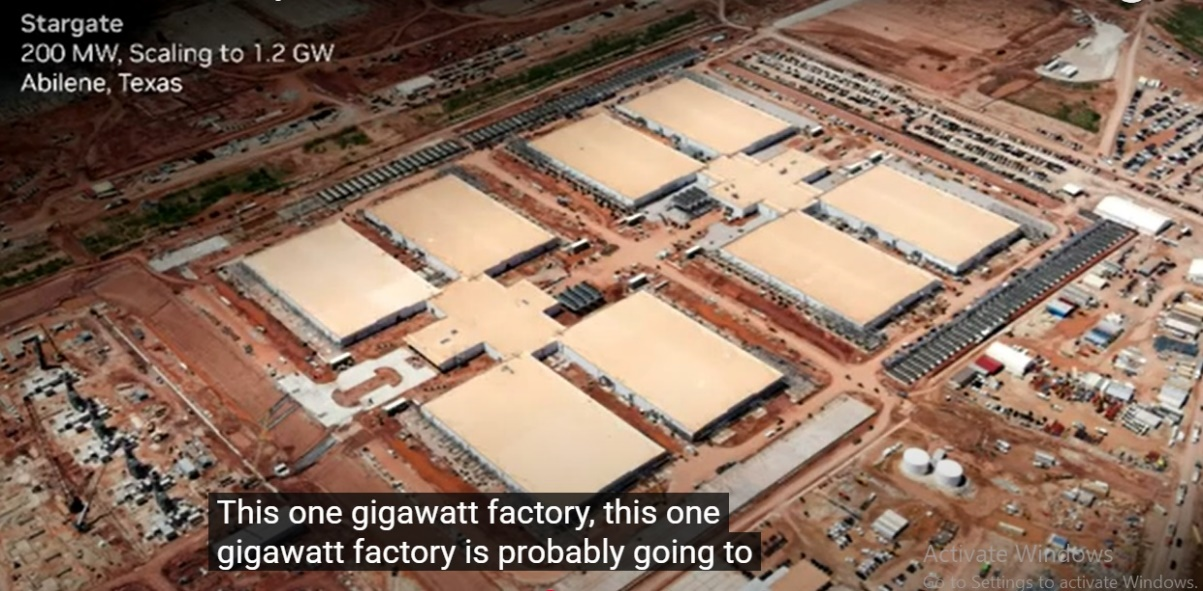
“This picture shows the controversial Stargate AI Data Center — a 200MW facility currently scaling up to a 1.2GW AI factory in Abilene, Texas. It’s a massive $500 billion venture led by OpenAI, Oracle, and SoftBank.
Stargate is set to become a 1-gigawatt AI factory, with an estimated investment of $60–80 billion, including $40–50 billion dedicated to electronics and computing infrastructure. Can you imagine the scale of this monumental investment as the U.S. enters the AI industrial era?
The rationale behind building such factories is clear: the more you invest, the more you gain — even though the technology is highly complex. Similar trends are seen globally, such as the massive investments in Taiwan by TSMC, the world’s largest GPU chip manufacturer, and Foxconn, the world’s leading producer of GPU servers and AI factory hardware.”
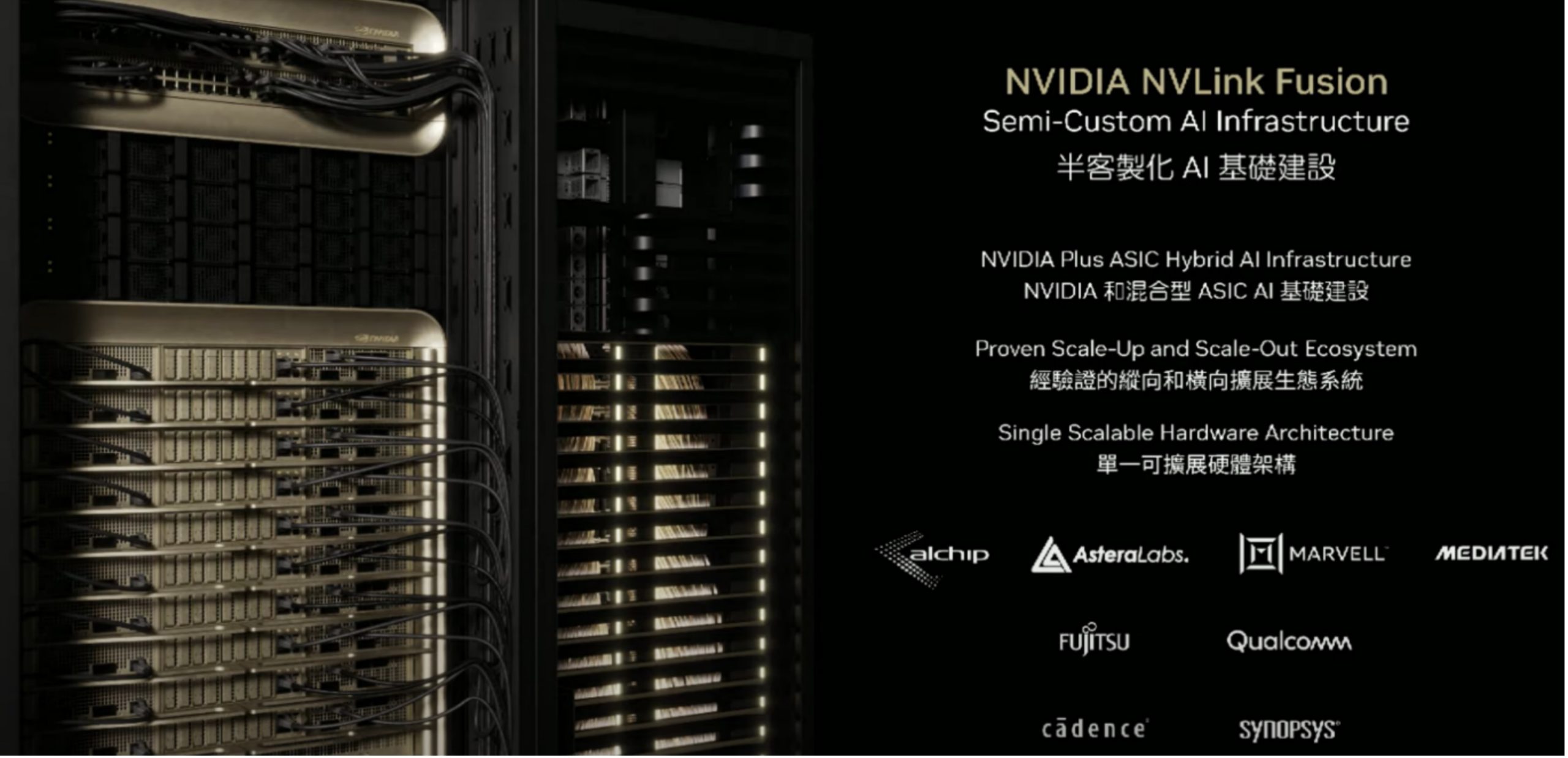
NVIDIA has formed strategic partnerships with several key players in the semiconductor and computing industry, including LCHIP, Astera Labs, Marvell, and MediaTek, as well as major hyperscale companies. The company is also collaborating with Fujitsu and Qualcomm, who are developing their own CPUs that integrate with the NVIDIA ecosystem via NVLink.
Additionally, NVIDIA is working closely with Cadence and Synopsys to license and transfer its intellectual property (IP), enabling broader industry adoption and seamless integration into partner designs.
Global & Taiwan Industrial Physical AI
Jensen Huang projects that companies around the world are in the midst of building over $5 trillion worth of factories. Optimizing the design and operation of these facilities is crucial to maximizing productivity and efficiency.
In Taiwan, industry leaders such as TSMC, Foxconn, Wistron, Pegatron, Delta Electronics, Quanta, GIGABYTE, and others are leveraging NVIDIA Omniverse to create digital twins—virtual replicas of physical factories. These digital twins are powering the next wave of industrial physical AI, revolutionizing semiconductor and electronics manufacturing by enabling real-time simulation, automation, and intelligent optimization.
Taiwan’s Foxconn, TSMC, NSTC, and NVIDIA to Build a World-Class AI Supercomputer
Taiwan isn’t just building AI GPU supercomputers for the world—it’s building one with the world. At COMPUTEX 2025, NVIDIA CEO Jensen Huang announced a major initiative: Foxconn, the Taiwanese government (via NSTC), TSMC, and NVIDIA will collaborate to build Taiwan’s first large-scale AI supercomputer, designed to power the nation’s AI infrastructure and ecosystem.
This initiative aims to support a broad spectrum of stakeholders—including AI researchers, scientists, students, startups, and major corporations like TSMC and Foxconn, both of which are deeply involved in advanced AI and scientific computing. Foxconn, for example, has extensive operations in robotics, which would greatly benefit from such cutting-edge infrastructure.
Establishing a world-class AI supercomputing hub in Taiwan is not just strategic—it’s essential. It enables NVIDIA to co-develop massive AI supercomputer chips and advanced NVLink connectivity technologies directly within a local ecosystem designed for innovation at scale.
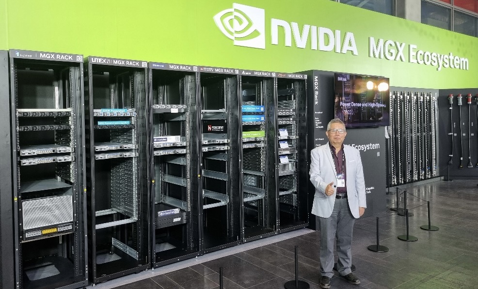
Several Taiwanese tech giants—Pegatron, QCT, Foxconn, GIGABYTE, and ASUS—are showcasing advanced GPU systems designed specifically to harness the full potential of NVIDIA’s Blackwell chips, effectively combining them into a single massive compute unit using NVLink technology. What’s often understated is the enormous complexity of the system architecture and the depth of the software ecosystem required to interconnect these components. This achievement is the result of collaboration among more than 150 Taiwanese companies across sectors including technology, software, and manufacturing, working together over just three years to build a fully integrated platform. It represents not just a technical breakthrough, but a massive industrial investment. And now, thanks to this ecosystem, anyone aiming to build an AI data center can do so—by deploying NVIDIA GB200s, GB300s, or other accelerated computing systems—powered by the same scalable infrastructure pioneered in Taiwan.
NVIDIA NVLink Fusion: Building the Future of Semi-Custom AI Infrastructure
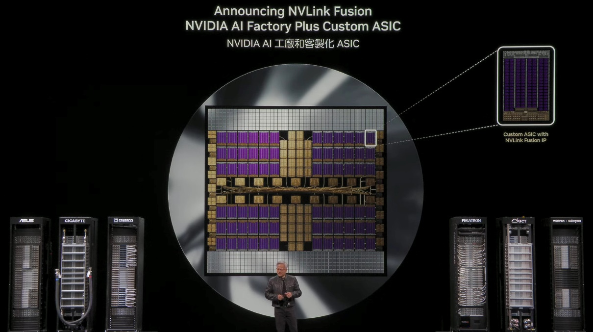
With NVIDIA NVLink Fusion, organizations can now build semi-custom AI infrastructures tailored to their specific workloads—some optimized with more CPUs, others with NVIDIA GPUs or even custom ASICs (Application-Specific Integrated Circuits).
The breakthrough lies in NVLink, NVIDIA’s high-bandwidth, low-latency interconnect, which allows these hybrid systems to scale up and function as powerful unified computers. NVLink is now available as a flexible architectural ingredient that anyone can integrate into their own designs.
Here’s how NVLink Fusion works: It enables the construction of an end-to-end NVIDIA AI supercomputing platform—including NVIDIA GPUs, CPUs, NVLink chiplets and switches, TPUs, and networking solutions such as Spectrum-XEthernet or InfiniBand NICs. Even if you use a third-party CPU or ASIC, NVIDIA provides chip-to-chip NVLink interfaces to connect seamlessly with Blackwell GPUs—or future architectures like Reuben.


